|
The Intel 4004 Microprocessor and the Silicon Gate Technology
|
|
|
A testimonial from Federico Faggin, designer of the 4004 and developer of its enabling technology
|
|
The Buried Contact
Faggin invented the buried contact in 1968 at Fairchild and made buried contact devices that same year. The
buried contact is a method to make direct ohmic contact between the polysilicon
gate material and the junctions, in silicon-gate integrated circuits. With this
method requiring an additional masking layer it was possible to use the
polysilicon as an additional layer of interconnection, greatly improving the
circuit density, particularly in random logic circuits.
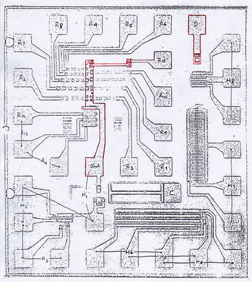
This photomicrograph shows the XTPG; the original test pattern designed
in 1968 by Federico Faggin at Fairchild Semiconductor to test the
critical parameters of devices built using the silicon gate technology.
The device marked D is a polysilicon to silicon diode and the device
marked R11 is a resistor whose connections are made with polysilicon to
silicon contacts. The red outline is intended to more clearly illustrate
the polysilicon to silicon contact (later called "buried contact") and the polysilicon to silicon diode.
The buried contact was invented by Faggin at Fairchild Semiconductor,
and was communicated to Leslie Vadasz, Faggin's supervisor at Fairchild, in
early March, 1968. In July, 1968, Vadasz joined Intel working for Andy Grove and later used and
patented under his name Faggin's invention.
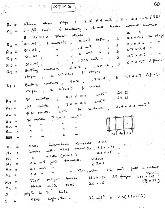
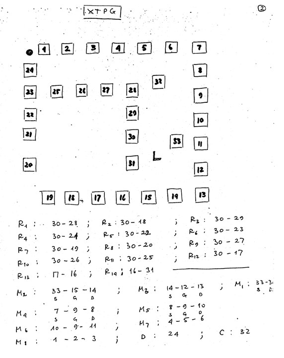
These two pages are the original description handwritten by Federico Faggin of the various experimental test patterns included in the XTPG chip.
|

|
|


