|
The Intel 4004 Microprocessor and the Silicon Gate Technology
|
|
|
A testimonial from Federico Faggin, designer of the 4004 and developer of its enabling technology
|
|
Original Schematics of the Intel 4004 Microprocessor
With introductory note on the creation of the first microprocessor
Definition of Microprocessor:
Microprocessor is the name for the central processing unit of a computer (CPU) integrated into a single chip of silicon. In the late 1960s microprocessors were considered to be a future possibility, and a few companies were developing CPUs partitioned in several chips. However, only a single-chip CPU could achieve the speed, power dissipation and cost necessary to address many applications; and in 1970 the microprocessor was still a dream.
The Problem:
The difficulty was not in defining the architecture or doing the logic design of a small CPU, which were well known, but in devising how to design all the needed circuits to be fast, with low power dissipation, and small enough to fit in a single chip that could be manufactured at low cost.
The Key Inventions that Made the 4004 Possible:
The MOS Silicon Gate Technology (SGT)
The SGT was created at Fairchild Semiconductor in 1968 by Federico Faggin who also designed the worlds first integrated circuit using SGT (the Fairchild 3708). This technology used self-aligned gates made of polycrystalline silicon, and could integrate twice as many random-logic transistors with 5 times higher speed than the incumbent technology. This was just enough advancement to make a microprocessor possible.
The SGT-Based Random Logic Design Methodology
In April, 1970 Faggin was hired by Intel to lead the design of the MCS-4 chip-family. This chip set had been specified jointly by Ted Hoff and Stan Mazor of Intel with the inputs of Busicom engineers, the first customer, to make a family of electronic calculators. However, in 1970 there was no methodology for random logic design with SGT.
The novel Silicon Gate Design Methodology that Federico Faggin conceived was based on a two-phase clock design with bootstrap loads and buried contacts, two key inventions of Faggin. Faggin also designed a number of basic circuit blocks and simple rules, based on graphic design, that allowed to rapidly size the transistor dimensions using load factors that could be determined with reasonable precision from a single schematic, since this document mirrored as closely as possible the layout plan of the chip. The single schematic made it possible to go directly from the chip specification to a design document that combined logic, circuit design and general transistor placement close to the layout, on one schematic. In this manner, the time required for the logic design, circuit design, and layout was minimized, and possible translation errors avoided.
The layout started with a grid of poly-silicon and aluminum lines carrying the key signals, and the actual circuits were then tucked underneath the grid, reflecting more or less the spatial location shown in the schematic. The result was a dense layout with a factor-of-two improvement in random-logic circuit density, and a factor of five in speed improvement, for the same power dissipation, compared with aluminum gate MOS technology with the same lithography. Furthermore, since SGT had junction leakage more than 100 times lower than metal gate, dynamic circuits had much better high temperature behavior than metal gate ICs.
Diagrams of the Original Schematics for the 4004
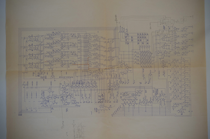
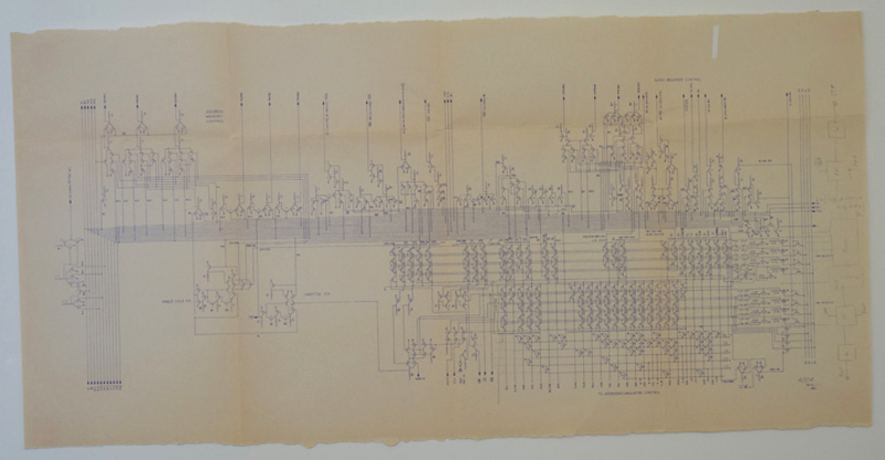
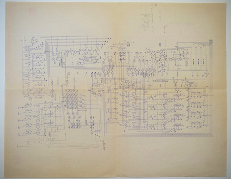
The following are photographs of Federicos original schematics for the 4004, in 3 sheets, with hand notations in pencil by Federico:

The Memory Block containing the index registers dynamic memory, address stack dynamic memory, program counter with incrementer, refresh counters, and effective address counter.

The Control Logic Block containing the instruction register, the instruction decoder, the control logic for the memory block, and the control logic for the arithmetic unit.

The Arithmetic Unit Block containing the adder/subtractor/shifter with decimal adjust, the accumulator and flag register, the internal bus control and the system timing.
|
The schematic diagrams show resistor symbols with either a B next to it or not. A resistor symbol actually indicates an MOS transistor with its gate connected to its drain and used as a resistive load. When a B symbol is shown, a bootstrap load needs to be used. The ratio of two numbers shown next to each resistor symbol indicates the width over length dimensions of the gate of the MOS transistor load. The active transistors all have a gate which is 9 microns long (unless explicitly indicated otherwise), and the number next to each transistor symbol is the width in microns of its gate. The minimum line width was 6 micrometer.
|
|
|

